Key Applications and Selection Guide for Industrial Lenses in Semiconductor Manufacturing
The semiconductor industry is the core pillar of modern science and technology, and industrial lenses, as the “eyes” in the semiconductor manufacturing process, play an indispensable role in quality control, precision testing, and automated production. This article will explore the various application scenarios of industrial lenses in the semiconductor field and provide specific lens selection recommendations.
The Importance of Industrial Lenses in Semiconductor Manufacturing
Semiconductor manufacturing is one of the most precision-demanding industrial processes in the world today, and the line width has entered the nanometer level (such as 3nm, 5nm process). Under such precision requirements, industrial vision systems must be able to:
- Detect micron or even nano-level defects
- Real-time monitoring on high-speed production lines
- Adapt to harsh industrial environments (clean rooms, chemical vapors, etc.)
- Handle complex surfaces with high reflectivity and low contrast
Main application scenarios and lens selection
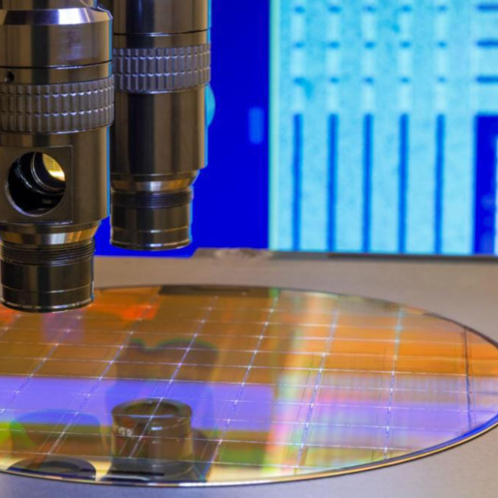
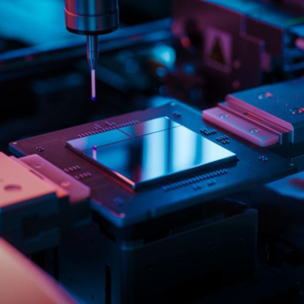
1.Wafer inspection
Application scenarios:
- Wafer surface defect detection (scratches, particle contamination, pattern defects)
- Alignment mark recognition
- Edge detection
Recommended lens types:
Telecentric lens: such as Fine-Lens’ telecentric lens series, which can eliminate perspective errors and ensure measurement accuracy
High-resolution fixed-focus lens: such as Fine-Lens’ FA lens series, suitable for subtle defect detection
Ultraviolet (UV) lens: used to detect transparent films and certain special materials; Fine-Lens’ UV lens series can be consulted with customer service to obtain specifications.
2.Chip packaging inspection
Application scenarios:
- Ball inspection (BGA, CSP)
- Wire bonding quality inspection
- Package appearance inspection
- Mark recognition (OCR)
Recommended lens types:
Zoom lens: such as Fine-Lens zoom lens, adapted to different package sizes
Large depth of field lens: such as Fine-Lens telecentric or tilt-shift series, to solve the problem of inconsistent height package component inspection
Infrared lens: used to inspect internal bonding wires
3.Lithography alignment
Application scenarios:
- Alignment of the mask and the wafer
- Measurement of overlay error
- Recommended lens types:
High-precision telecentric lens: such as Fine-Lens telecentric lens series, distortion <0.1%
UV transmission lens: for a deep ultraviolet (DUV) lithography system
4.PCB board inspection
Application scenarios:
- Pad inspection
- Line defect inspection
- Component mounting position inspection
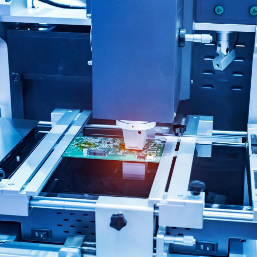
Recommended lens types:
Line scan lens: such as Fine-Lens line scan lens series, suitable for high-speed PCB inspection
Large target lens: such as the Fine-Lens large target lens series, can capture a large area at one time.
Special application scenarios
- Transparent material inspection
Application scenarios: Glass wafer, photomask inspection
Solution:
- Use a special polarization lens to reduce reflection
- With a coaxial lighting system
- 3D inspection
Application scenarios:
- Chip bump height measurement
- Package thickness inspection
Solution:
- Laser confocal microscope lens
- Structured light 3D imaging system
- High temperature environment detection
Application scenario: Wafer heat treatment process monitoring
Solution:
- High-temperature resistant lens
- Used with a cooling protective cover
Key selection parameters
When selecting industrial lenses for semiconductors, consider:
- Resolution: Need to match the camera pixel size, generally 1-2μm/pixel
- Working distance: Limited by equipment space
- Depth of field: Significant for uneven surfaces
- Distortion: Telecentric lenses are usually <0.1%
- Spectral response: UV, visible light, or infrared
- Environmental adaptability: Dustproof, chemical corrosion resistance, etc.
Future trends
- Higher resolution: As process nodes shrink, lens systems that can distinguish nanoscale features are required
- Multi-spectral imaging: Combine different bands to improve the defect detection rate
- AI-assisted detection: High-resolution lenses provide better image data for AI algorithms
- Online real-time detection: High-speed lenses combined with high-performance processors achieve 100% full inspection
Conclusion
In the semiconductor industry, a precision industry with “nanometers” as units, the choice of industrial lenses directly affects product quality and production efficiency. The right lens solution can not only improve the defect detection rate but also reduce the misjudgment rate and production downtime. As semiconductor technology continues to advance, industrial lens technology will continue to innovate, providing strong support for the continuation of Moore’s Law.
For semiconductor manufacturers, working with professional industrial lens suppliers and technical teams to customize optical solutions according to specific application scenarios will be one of the key factors to enhance competitiveness. We welcome all semiconductor manufacturers to cooperate with us at Fine-Lens for mutual benefit.