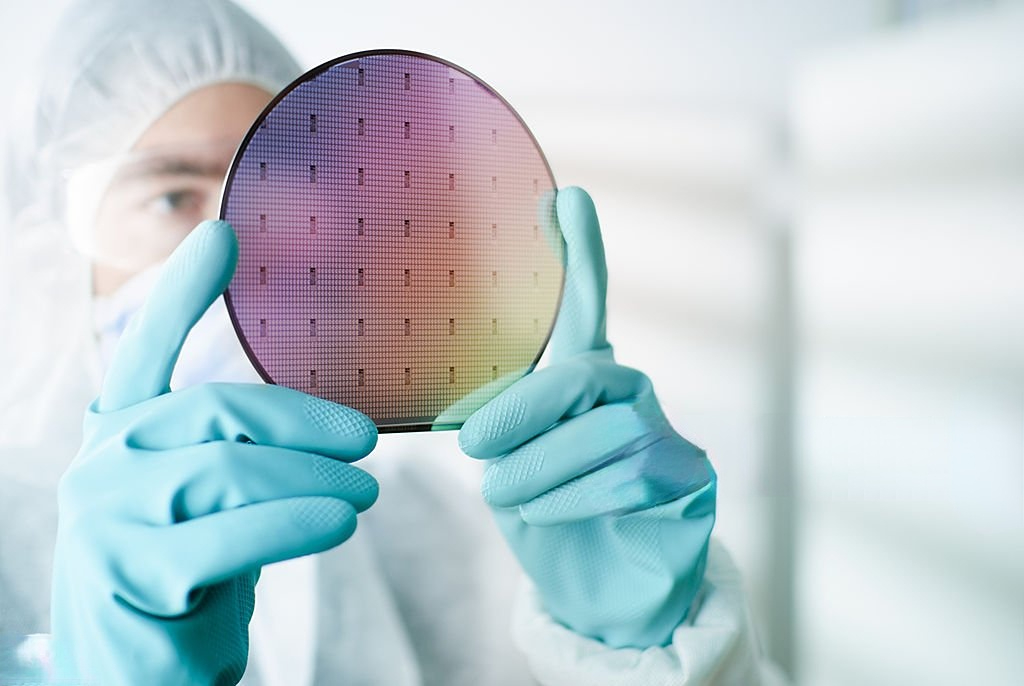
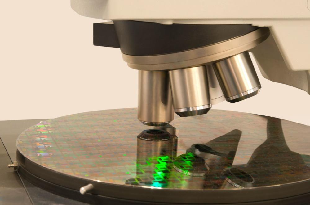
Industrial lenses play an important role in semiconductor inspection and are mainly used for high-precision imaging of wafer surfaces. They ensure the quality and performance of semiconductor products by capturing tiny defects, size, shape and other details on the wafer surface. Industrial lenses with high resolution, high contrast and high optical performance can provide clear and accurate image data, providing reliable technical support for semiconductor inspection.
There are many types of industrial lenses used for semiconductor inspection. The following is a detailed introduction to these lenses:
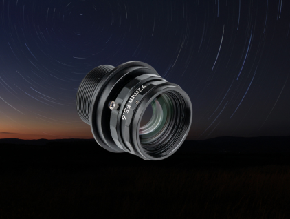
1.Variable-Magnification Industrial Lens
Features: The magnification can be adjusted continuously and infinitely within a certain range, with high contrast and high-resolution imaging capabilities.
Advantages: The magnification can be adjusted to adapt to wafer inspection of different sizes, improving the flexibility and adaptability of the system. At the same time, high-precision variable-magnification industrial lenses can provide more accurate inspection results
2.Telecentric Lens
Features: The magnification is constant and does not change with the change of working distance, which can eliminate the parallax of traditional industrial lenses.
Application: Commonly used for precision measurement and detection tasks in semiconductor and electronic equipment manufacturing, such as wafer detection, chip packaging, etc.
Advantage: It can ensure that objects of the same size and different distances obtain images of the same size on the imaging surface, thereby improving the accuracy and reliability of measurement
3.High-resolution fixed-focus lens
Features: Constant focal length, field of view changes with working distance, suitable for scenes where working distance is fixed and the detection area is on the same plane.
Advantages: Can provide high-resolution images, clearly capture details and defects on the wafer surface, and ensure detection accuracy
In addition, there are other types of industrial lenses that are also widely used in the field of semiconductor inspection, such as:
Line Scan Lens: Commonly used for high-speed, high-precision continuous inspection, such as continuous scanning inspection of the wafer surface.
Macro Lens: Has a large magnification ratio and can be used to shoot smaller objects, such as tiny structures on chips.
Zoom Lens: Can achieve focal length transformation, so as to obtain different widths and narrows of viewing angles, suitable for inspection scenarios that require flexibility but low resolution requirements.
These lenses play a vital role in semiconductor inspection. They can meet the needs of different inspection scenarios and improve inspection efficiency and accuracy.
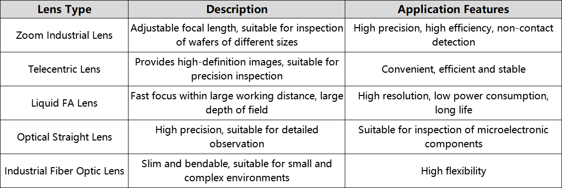
Industrial Lens Types for Semiconductor Inspection:
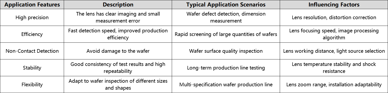
Application characteristics of industrial lenses in semiconductor inspection: