Revolutionizing UV Printing with Telecentric Lenses
The evolution of UV printing—spanning industrial 3D manufacturing, PCB lithography, and high-precision material processing—demands optical systems capable of extreme resolution, minimal distortion, and unwavering stability under intense UV energy. At the heart of this transformation lies a critical component: the telecentric lens. Fine-Lens’ 4K7μ telecentric lens (4K resolution, 7μm pixel tolerance) emerges as a benchmark for next-generation UV printing, enabling breakthroughs in accuracy, speed, and reliability.

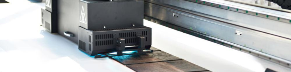
Fine-Lens 4K7μ Telecentric Lens applies in UV Printer
The UV Printing Revolution & Optical Challenges
UV printing leverages ultraviolet light to cure resins, etch materials, or project micro-patterns with micron-level precision. Applications range from:
- 3D printing
- PCB lithography (direct imaging for circuit patterns)
- Laser material processing (wafer dicing, display annealing)
Key challenges for optical systems include:
- Thermal stress: High-power UV light degrades conventional lenses, causing focus drift and coating delamination
- Distortion control: Sub-μm pattern fidelity requires lenses with near-zero geometric distortion to avoid misalignment in multi-layer printing.
- Spectral precision: Lenses must maintain clarity across UV spectra (e.g., 340–420 nm) without chromatic aberration.
Why Telecentric Lenses? The Fine-Lens 4K7μ Advantage
Telecentric lenses eliminate perspective error and ensure consistent magnification across varying working distances—critical for maintaining edge acuity in UV-printed patterns. Fine-Lens’ 4K7μ lens amplifies this with:
1.Ultra-High Resolution & Pixel Matching
- 4K (3840 × 2160) resolution aligned to DLP670S/DLP9500UV chipsets, supporting <10μm feature replication—ideal for semiconductor lithography and micro-3D printing.
- 7μm pixel tolerance ensures no detail loss, even with Sony IMX487 UV sensors (2.74μm pixel size).
2.Zero Distortion for Critical Alignment
- <0.01% distortion prevents “pattern drift” in multi-pass printing, crucial for PCB layer stacking and OLED display repair.
- Matches or exceeds performance of specialized UV lenses.
3.UV-Optimized Materials & Coatings
- Fluorite glass elements minimize chromatic aberration across 280–420 nm, outperforming standard SiO₂ lenses in edge contrast.
- Low-outgassing coatings resist fogging under high-energy UV exposure, extending service life in 24/7 printing environments.
4.Thermal Stability for High-Power Systems
- Stainless-steel housing dissipates heat from UV lasers (e.g., 100W pulsed sources), preventing focal shift during continuous operation.
- Maintains optical alignment under 30G vibrations—critical for conveyor-based printing lines.
Transforming Applications: Case Examples
1. Industrial 3D Printing
- Problem: Consumer-grade lenses degrade after hours under high-intensity UV (6.5W+), causing failed prints and downtime.
- Solution: Fine-Lens 4K7μ paired with DLP670S chips ensures uniform light distribution across large build areas (195 × 122 mm), enabling 8K-equivalent projection for aerospace/composite parts.
2. Semiconductor Direct Imaging
- Problem: UV lens distortion >0.05% misaligns circuit patterns, increasing wafer scrap rates.
- Solution: Near-zero distortion and 7μm resolution allow 1:1 pattern transfer for <2μm line widths, boosting yield by up to 20%.
3. High-Speed Material Marking
- Problem: Thermal expansion in aluminum-housed lenses blurs marks during high-throughput processing.
- Solution: Low-thermal-drift design maintains focus over 150+ hours of continuous 355-nm laser marking.
Integration Insights: Maximizing System Performance
Pair Fine-Lens 4K7μ with complementary technologies for peak results:
- Sensors: Sony IMX487 UV sensors (813 million pixels) for defect detection during printing.
- Light Engines: TI DLP9500UV chips (48Gbps data rate) for rapid pattern switching.
- Beam Delivery: Low-outgassing UV F-Theta lenses for scan-head synchronization.
Pro Tip: For multi-wavelength systems (e.g., UV+IR curing), specify our anti-reflective coating variant to suppress ghosting.
The Future: Where Fine-Lens Leads Next
As UV printing advances toward nanoscale features (e.g., sub-1μm semiconductor vias) and faster throughput (1,000+ layers/hour), Fine-Lens is pioneering:
- Multi-spectral telecentric lenses: Single-lens solutions spanning UV to NIR (250–1000 nm) for hybrid printing/inspection systems.
- AI-driven calibration: Auto-compensation for thermal drift/vibration in real time.
Conclusion: Precision as Standard
In UV printing’s high-stakes arena—where micron-scale errors cost thousands—Fine-Lens’ 4K7μ telecentric lens delivers uncompromising optical performance. By marrying zero distortion, UV-hardened durability, and 4K resolution, it transforms theoretical precision into production reality.
*Learn how our 4K7μ lens integrates into your UV printing platform: [Contact Fine-Lens for technical white papers and integration kits]*